 24-hour service hotline: 0513-85708666

An important guarantee for chip yield, and the domestic replacement of semiconductor cleaning equipment is timely
01Cleaning equipment: the cleaning steps run through all aspects of chip production, and wet cleaning is the mainstream technology
1.1 The cleaning process runs through all aspects of chip production and is an important guarantee for chip yield
Cleaning is an important part of semiconductor manufacturing process and one of the most important factors affecting the yield of semiconductor devices.
Cleaning is an important step in the wafer processing and manufacturing process. In order to minimize the impact of impurities on the chip yield, in the actual production process, it is not only necessary to ensure efficient single cleaning, but also necessary to carry out frequent cleaning before and after almost all processes. It is a necessary link in the key processes such as monocrystalline silicon wafer manufacturing, photolithography, etching and deposition.
1)In the manufacturing process of silicon wafers, the silicon wafers after polishing treatment need to be cleaned to ensure the flatness and performance of their surfaces, so as to improve the yield in subsequent processes.
2)During the wafer manufacturing process, the wafer needs to be cleaned before and after the key processes such as photolithography, etching, ion implantation, degumming, film formation and mechanical polishing, so as to remove the chemical impurities contaminated by the wafer, reduce the defect rate and improve the yield.
3)In the process of chip packaging, the chip needs TSV (silicon perforation) cleaning, UBM / RDL (bump bottom metal / film redistribution Technology) cleaning and bonding cleaning according to the packaging process.
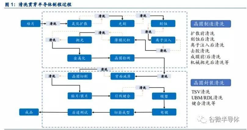
Before entering each process, the surface of the silicon wafer must be clean. It needs to undergo repeated cleaning steps to remove the pollutants on the surface.Chip manufacturing needs to be carried out in a dust-free room. In the process of chip manufacturing, any contamination will affect the normal function of devices on the chip. Contamination impurity refers to any substance introduced in the semiconductor manufacturing process that endangers the chip yield and electrical performance. Specific contaminants include particles, organic matter, metal and natural oxide layer, etc. such contaminants include the environment, other manufacturing processes, etching by-products, grinding fluid, etc. If the above contamination impurities are not cleaned in time, it may lead to the failure of subsequent processes, lead to electrical failure, and eventually cause the chip to be scrapped.
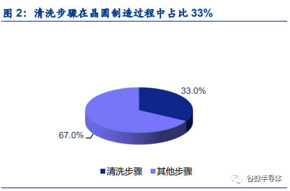
The number of cleaning steps is the process with the largest proportion of chip manufacturing process steps, accounting for more than 30% of all chip manufacturing process steps. With the progress of semiconductor manufacturing technology nodes, the number and importance of cleaning processes will continue to increase。After the semiconductor chip process technology node enters 28nm, 14nm and more advanced levels, the process flow is prolonged and more complex, and the yield of the production line will also decrease. One reason for this phenomenon is that the advanced process is more sensitive to impurities, and it is more difficult to clean small-scale pollutants efficiently. The solution is to increase the cleaning steps. Each wafer requires even more than 200 cleaning steps in the whole manufacturing process, and wafer cleaning becomes more complex, important and challenging.
1.2. Wet cleaning is the mainstream cleaning technology
According to different cleaning media, cleaning technology can be divided into wet cleaning and dry cleaning. Wet cleaning refers to the use of solution, acid, alkali, surfactant, water and their mixtures, through corrosion, dissolution, chemical reaction and other methods, to make impurities on the surface of silicon wafers react with the solvent to produce soluble substances, gases or directly fall off, so as to obtain silicon wafers that meet the requirements of cleanliness. Dry cleaning refers to cleaning technology that does not rely on chemical reagents, including plasma cleaning and meteorological cleaning& nbsp; Wet cleaning is usually used in the wafer manufacturing line, which is the mainstream cleaning method in the current market.
1.2.1 wet clean
Wet cleaning uses liquid chemical reagents and DI water to oxidize, etch and dissolve the surface pollutants, organic matters and metal ions on the wafer. The commonly used wet cleaning methods include RCA cleaning method, dilution chemical method, IMEC cleaning method and single crystal cleaning method.
1) RCA general cleaning method: RCA cleaning method relies on solvent, acid, surfactant and water to spray, purify, oxidize, etch and dissolve the surface pollutants, organic matters and metal ions on the wafer without damaging the surface characteristics of the wafer. Clean thoroughly in ultrapure water (UPW) after each use of chemicals.

2) Chemical dilution method: on the basis of RCA cleaning, the use of dilution chemical method for SC1 and SC2 mixture can greatly save the consumption of chemicals and DI water. And H2O2 in the SC2 mixture can be completely removed. Dilution of APM SC2 mixture (1:1:50) can effectively remove particles and hydrocarbons from the wafer surface. Strongly diluted HPM mixture (1:1:60) and diluted HCI (1:100) can be as effective as standard SC2 liquid when removing metals. Another advantage of using diluted HCI solutions is that particles do not precipitate at low HCI concentrations. The diluted RCA cleaning method can reduce the total chemical consumption by 86%. After diluting SC1, SC2 solution and HF replenishing megasonic agitation, the service temperature of the solution in the tank can be reduced, and the time of various cleaning steps can be optimized. Therefore, the service life of the solution in the tank is prolonged, and the chemical consumption is reduced by 80-90%. The experiment shows that the UPW consumption can be reduced by 75-80% by using hot UPW instead of cool UPW. In addition, a variety of diluted chemical liquids can greatly save washing water due to low flow rate or cleaning time requirements.
3)IMEC cleaning method:
①In the first step, organic pollutants are removed to form a thin layer of chemical oxide to effectively remove particles. Sulfuric acid mixtures are usually used。
②In the second step, the oxide layer is removed, and the particles and metal oxides are removed at the same time. Cu, Ag and other metal ions will deposit on the Si surface when they exist in HF solution. The deposition process is an electrochemical process, and the surface deposition rate of copper is accelerated under the illumination condition.
③The third step is to generate hydrophilicity on the silicon surface to ensure that no dry spots or watermarks are generated during drying. The diluted HCl / O3 mixture is usually used to make the silicon surface hydrophilic at low pH value and avoid metal pollution. The concentration of HNO3 is increased in the final rinsing process to reduce CA surface pollution.
3) Single wafer cleaning: the above method is not good to ensure the completion of the cleaning process for large-diameter wafers, and the single wafer cleaning method is usually used. The cleaning process is to reuse di-o3 / DHF cleaning solution at room temperature, ozonized DI water (di-o3) generates silicon oxide, dilute HF etches silicon oxide, and remove particles and metal pollutants at the same time. According to the requirements of etching and oxidation, a short spraying time can obtain a good cleaning effect without cross contamination. Finally, either DI water or ozonized DI water is used for flushing. In order to avoid water stains, isopropyl alcohol (IPA) with a large amount of nitrogen is used for drying treatment. Wafer cleaning has better cleaning effect than the improved RCA cleaning. DI water and HF are recycled in the cleaning process to reduce the consumption of chemicals and improve the cost-effectiveness of wafers.
1.2.2 Dry cleaning
Dry cleaning uses the gas phase method to remove the contaminants on the wafer surface. Gas phase chemical methods mainly include thermal oxidation method and plasma cleaning method. The cleaning process is to introduce thermal chemical gas or plasma reaction gas into the reaction chamber. The reaction gas reacts with the wafer surface to generate volatile reaction products, which are evacuated by vacuum. Annealing in CI containment environment is a typical thermal oxidation process, which is carried out in an oxidation furnace. Argon (AR) sputtering is usually carried out on site before sputter deposition. The advantage of dry cleaning is that there is no waste liquid after cleaning, and local treatment can be carried out selectively. In addition, the anisotropy of dry cleaning etching is conducive to the formation of thin lines and geometric features. However, the gas-phase chemical method can not selectively react only with the surface metal pollutants, and inevitably react with the silicon surface. The evaporation pressure of various volatile metal mixtures is different, and the volatility of various metals is different at low temperature. Therefore, under certain temperature and time conditions, all metal pollutants cannot be completely removed. Therefore, dry cleaning cannot completely replace wet cleaning. The experiments show that the metal pollutants that can be reduced by the gas phase chemical method according to the required standards include iron, copper, aluminum, zinc, nickel, etc. in addition, the chemical method based on Cl ions can also effectively volatilize calcium at low temperature. Dry and wet cleaning methods are usually used in the process.
1.3. Single chip cleaning has high yield and is the current mainstream cleaning equipment
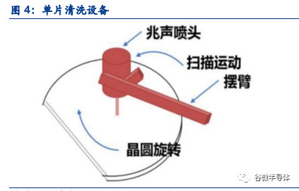
Under the technical route of wet cleaning, cleaning equipment can be divided into single-chip cleaning equipment, trough cleaning equipment, batch rotary spray cleaning equipment and scrubber, among which single-chip and trough cleaning equipment are the mainstream cleaning equipment at present. Single wafer cleaning is to send each wafer to each cavity for separate spray cleaning, which is easy to control the cleaning quality and improve the cleaning uniformity of different positions of the single wafer, but the disadvantage is low cleaning efficiency. Trough cleaning is to put multiple wafers (100-200 wafers) into the cleaning tank for centralized cleaning. Such cleaning equipment has high efficiency and low cost, but the disadvantage is that the concentration is difficult to control and cross contamination may occur.
At present, single chip cleaning has gradually replaced groove cleaning in the advanced process of integrated circuit manufacturing and become the mainstream. The main reasons include: (1) single chip cleaning can provide better process control and improve product yield; (2) In the case of larger size wafers and more advanced processes, which are more sensitive to impurities, cross contamination in tank cleaning will endanger the yield of the whole batch of wafers and bring high cost chip rework expenses; (3) The appearance of single-chip tank combined cleaning technology can improve the cleaning capacity and efficiency, reduce the use of sulfuric acid, and help customers effectively reduce costs. (report source: future think tank) 报错 笔记
02Semiconductor equipment enters an upward cycle, and advanced technology brings new growth to cleaning equipment
2.1. The semiconductor market is booming, and the rising capital expenditure drives the high growth of the equipment market
Driven by the demand for 5g, Internet of things, automotive electronics and cloud computing, the semiconductor market demand continues to grow. In 2020, despite the impact of the epidemic, the global semiconductor market scale still increased by 6.8% year-on-year, reaching US $440.4 billion. It is estimated that the global semiconductor market scale in 2021 and 2022 will be US $527.2 billion and US $573.4 billion respectively, up 19.7% and 8.8% year-on-year respectively. From the perspective of sub regions, the growth rate of the Asia Pacific market is higher than the global average, with 23.5% and 9.2% respectively, accounting for 63% and 64% of the global market respectively.
The increase in capital expenditure of semiconductor manufacturers will drive the rapid growth of equipment market scale. According to semi statistics, the global semiconductor equipment market scale will increase from US $31.8 billion in 2013 to US $71.2 billion in 2020, with a compound annual growth rate of 12.21%, and a year-on-year growth of 19.15% in 2020. It is expected that the global semiconductor equipment market will increase to US $95.3 billion in 2021, with a year-on-year increase of 33.85%, and exceed US $100 billion in 2022. In addition, China's semiconductor equipment sales increased from US $3.3 billion in 2013 to US $18.7 billion in 2020, with a compound annual growth rate of 27.70%, far exceeding the growth rate of the global market.
2.2. The proportion of mainland wafer production capacity continues to increase, which is expected to drive the growth of domestic equipment demand
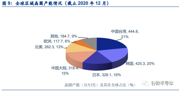
Driven by the strong support of national policies and the booming industry, semiconductor enterprises in the mainland have increased their capital expenditure one after another. According to IC insights, as of December 2020, the wafer production capacity of Chinese Mainland was 3.18 million pieces / month (equivalent to 8 inches), accounting for 15.3% of the world. IC insights further pointed out that as the capacity of semiconductor manufacturing silicon wafers continues to transfer to China, it is expected that the proportion of capacity will increase to 18% by 2025, and it is the only region with increased capacity share from 2020 to 2025.
According to semi's data, global semiconductor manufacturers will build 19 and 10 new wafer plants in 2021 and 2022 respectively, among which, mainland China and Taiwan, China each have 8 new wafer plant construction plans, followed by 6 in the Americas, 3 in Europe / Middle East, and 2 in Japan and South Korea. The equipment expenditure of these 29 wafer plants is expected to exceed 140 billion US dollars in the next few years. Chinese Mainland has a large investment plan in semiconductor plants, which is expected to greatly drive the demand for domestic equipment in the upstream.
2.3 Cleaning equipment has a large market space, and single-chip equipment will occupy a dominant position for a long time
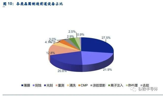
Semiconductor manufacturing equipment generally includes photolithography, etching, thin film deposition, both sides, cleaning, CMP and other equipment. According to Gartner data, cleaning equipment accounts for more than 4% of wafer manufacturing equipment.
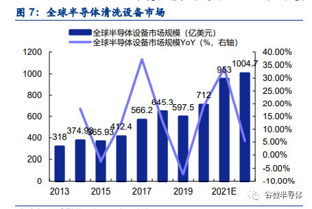
According to Gartner data, the global market scale of semiconductor cleaning equipment was US $3.42 billion in 2018. In 2019 and 2020, due to the decline of the global semiconductor industry and the impact of the COVID-19 epidemic, the global market scale of semiconductor cleaning equipment decreased to US $3.05 billion and US $2.54 billion respectively. It is expected that in 2021, with the recovery of the global semiconductor industry and the promotion of the global semiconductor equipment market scale, the semiconductor cleaning equipment market will show an annual growth trend, and the global semiconductor cleaning equipment market scale will reach US $3.2 billion in 2024.
Slave structureAccording to Gartner's data, the market share of single-chip cleaning equipment, trough cleaning equipment, batch rotary spray cleaning equipment and washer and other types of cleaning equipment in 2019 were US $2.276 billion, US $552 million, US $13 million and US $208 million, respectively, accounting for 74.63%, 18.10%, 0.44% and 6.83%. With the further reduction of the characteristic size of integrated circuits, the single-chip cleaning equipment will be more widely used in the process below 40nm, and the proportion is expected to gradually increase in the future. According to the prediction of Tokyo electronics, single chip cleaning will occupy the main market share for a long time.
2.4 Advanced technology adds new growth opportunities for cleaning equipment
In addition to benefiting from the rising business cycle of the semiconductor industry, the upgrading of the semiconductor process will also bring new growth opportunities for cleaning equipment. With the progress of the advanced chip manufacturing process and the complexity of the chip structure, the cleaning equipment market is expected to increase in volume and price.
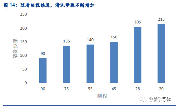
1) With the continuous progress of semiconductor technology, the integration of semiconductor devices continues to improve, and the cleaning steps are greatly improved. The 90nm chip cleaning process is about 90 times, and the 20nm chip cleaning process reaches 215 times. As the chip enters 16nm and below 7Nm, the number of cleaning processes will accelerate.
2)On the other hand, the size of semiconductor wafers is constantly expanding. The size of mainstream wafers has grown from 4 inches and 6 inches to 8 inches and 12 inches at the present stage. In addition, the structure of semiconductor devices tends to be complicated. For example, NAND flash memory in the memory field, according to the international semiconductor technology roadmap, when the process size reaches 14nm, the current flash memory technology will reach the limit of size reduction, and the memory technology will shift from two-dimensional to three-dimensional architecture, entering the 3D era. In the manufacturing process of 3dnand, the series memory cells in the original two-dimensional plane horizontal arrangement in 2dnand are mainly changed to vertical arrangement. By increasing the number of three-dimensional layers, the process problem that it is difficult to miniaturize on the plane is solved. The number of stacked layers is also developed from 32 and 64 to 128. The improvement of 3D storage technology puts forward higher requirements on the basis of cleaning the wafer surface, that is, cleaning the three-dimensional internal contamination without damage, which puts forward higher requirements on the cleaning equipment, and the value of the cleaning equipment will continue to rise.
03 Japanese manufacturers lead the cleaning equipment market, and domestic substitution is progressing smoothly
3.1. Japanese manufacturers take the lead in cleaning equipment, and domestic manufacturers' replacement is progressing smoothly
The global semiconductor cleaning equipment is highly concentrated in Japanese enterprises. According to Gartner data, the leading enterprises in the global semiconductor cleaning equipment industry are mainly Dainippon screen, Tokyo Electronics (TEL), Korean semes, Lam research, etc. Among them, deans is in the absolute leading position, accounting for 45.1% of the global market share of semiconductor cleaning equipment in 2020. Tokyo electronics, semes and Lam research respectively account for about 25.3%, 14.8% and 12.5%.
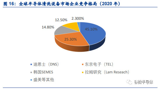
a)Dainippon screen: founded in 1943, headquartered in Tokyo, Japan, it is a Japanese semiconductor special equipment and LED production equipment company with customers in Japan, South Korea and Taiwan, China. The company's products mainly include semiconductor equipment, display equipment, PCB equipment, etc. Semiconductor equipment products mainly include cleaning machines, etching, developing / coating, etc. among them, cleaning equipment has a very high market share in the semiconductor industry. In 2020, the global market share exceeded 45%, ranking first in the world.
b)Tokyo electron: founded in 1963 and headquartered in Tokyo, Japan, it is the largest semiconductor manufacturing equipment supplier in Japan. It is mainly engaged in the RD, production and sales of semiconductor equipment. The products of Tokyo electron cover almost all processes in the semiconductor manufacturing process. Its main products include coating / imaging equipment, heat treatment film forming equipment, dry etching equipment, CVD, wet cleaning equipment and testing equipment. Its global share of cleaning equipment will reach 25.3% in 2020.
c)Lam research: founded in 1980 and headquartered in Fremont, California, USA, Lam research is one of the major suppliers of wafer manufacturing equipment and services to semiconductors worldwide. The company's main products include semiconductor processing equipment such as etching equipment, vapor deposition equipment, electroplating equipment and cleaning equipment for manufacturing integrated circuits. Its global share of cleaning equipment will reach 12.5% in 2020。
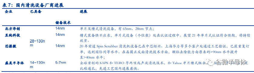
Important participants in China's semiconductor cleaning field include Zhichun technology, shengmei semiconductor, North Huachuang, Xinyuan micro, etc. although domestic semiconductor cleaning manufacturers started later than overseas, they have a strong momentum of catching up:
(1)Zhichun technology has 8-12 inch high-level single wafer wet cleaning equipment and trough type wet cleaning equipment. Its products cover many downstream applications such as wafer manufacturing, advanced packaging and solar energy. The company's wet process equipment has two types: trough type and monolithic type (8-12 reaction chamber), which can provide all wet processes to 28 nm nodes. It has been cut into SMIC international, Huahong group and other front-line users. The monolithic wet process equipment has won many orders from important domestic users.
(2)Shengmei semiconductor is the leader of domestic semiconductor cleaning equipment. It is in the leading position in the industry in 12 inch line cleaning equipment. It has a rich product line and the largest revenue volume of cleaning equipment in China. The main products of the company are single-chip cleaning equipment in the field of integrated circuits, including single-chip saps megasonic cleaning equipment, single-chip Tebo megasonic cleaning equipment, single-chip back cleaning equipment, single-chip front channel brushing equipment, slot cleaning equipment, single-chip slot combined cleaning equipment, etc.
(3)North Huachuang is the leader of domestic semiconductor equipment, with rich product lines, including etching machine, PVD, CVD, ALD, oxidation / diffusion furnace, annealing furnace and cleaning machine. The company has completed the cleaning equipment production line by acquiring American semiconductor equipment manufacturer akrion systems LLC. at present, the main cleaning equipment products of the company are single-chip and trough cleaning equipment, which can be applied to chip manufacturing with 65nm and 28nm technology nodes.
(4)At present, the main products of Xinyuan micro include coating and developing equipment (coating / developing machine, glue spraying machine) and single-chip wet equipment (cleaning machine, degumming machine and wet etching machine) in the photolithography process. The previous spin scruber cleaning machine produced by the company has reached the international advanced level and successfully realized import substitution. It has passed process verification at many customers such as SMIC international, Shanghai Huali and Xiamen Shilan Jike, And obtained batch repeated orders from many Fab manufacturers in China.
According to the information of China International Tendering network, based on the bidding purchase share of cleaning equipment of mainstream wafer factories in China from 2019 to 2021, the localization rate of semiconductor cleaning equipment in China has been maintained at 10% ~ 20%, breaking the fastest, and the localization rate has exceeded most other equipment. However, on the whole, there is still a big gap between domestic enterprises and international well-known enterprises in terms of scale, product technology strength and popularity. In the future, with the development of domestic semiconductor industry and the strong support of national policies, the domestic substitution trend is accelerating, and domestic cleaning equipment enterprises are expected to grow rapidly.
3.2. The second phase of the large fund will increase equipment investment, and the domestic substitution process is expected to accelerate
2In September 2014, the first phase of the national integrated circuit industry fund was established. According to incomplete statistics, the enterprises invested in the first phase of the large fund include: wafer manufacturer SMIC international, Changjiang storage, Shilan micro, etc., packaging and testing factory director electronics technology, Huatian technology, Tongfu micro, IC Design factory Ziguang group, nastar, Guoke micro, Zhongsheng technology network, xingmicroelectronics, Zhaoyi innovation, huiding technology, jingjiawei, etc; Equipment manufacturers: Zhongwei semiconductor, North Huachuang, Changchuan technology, etc; Material suppliers: Xinhua semiconductor, Xinsheng semiconductor, Anji microelectronics, Jacques technology, etc.
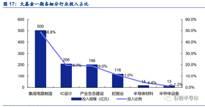
The second phase of the national large fund was registered and established on October 22, 2019, with a registered capital of 204.15 billion yuan. The second phase of the large fund is the continuation of the first phase, which is 45% larger than the first phase. According to the proportion of investment in subdivided industries in the first phase of the large fund, it can be seen that the first phase mainly focuses on the layout of major industrial links such as wafer foundry, design and sealing test, while the investment in semiconductor materials and equipment is less. We expect that the second phase will increase the investment in upstream equipment and materials, such as film equipment, testing equipment, cleaning equipment, chemical mechanical grinding equipment and other domestic equipment fields, as well as photoresist, target materials Silicon wafer and other semiconductor materials. According to the data of the second phase of the national large fund, the second phase of the large fund will focus on supporting the development of domestic equipment and materials from three aspects.
1) The phase II fund will maintain high-intensity and continuous support for enterprises that have been deployed in the fields of etching machine, film equipment, testing equipment and cleaning equipment, and cultivate enterprise seedlings of "Applied Materials" or "Dongdian Electronics" in Chinese Mainland. 2) Accelerate the investment layout of core equipment and key parts such as lithography machine and chemical mechanical grinding equipment, and fill the blank of domestic process equipment. 3) Urge manufacturing enterprises to improve the proportion of domestic equipment verification and procurement, and provide process verification conditions for more domestic equipment and materials.
From the recent actions of the second phase of the large fund, it has invested in domestic semiconductor equipment companies, including China micro company, North Huachuang, Zhiwei Technology (Zhichun technology subsidiary), Changchuan intelligent (Changchuan technology subsidiary), and the investment in equipment is significantly increased compared with the first phase. With the second phase of the national large fund increasing investment in upstream equipment and accelerating the domestic substitution trend of equipment, domestic equipment manufacturers will usher in a good opportunity for development.
04Analysis of key companies
4.1.To pure technology: the leader in cleaning the track, and the cleaning equipment has entered an accelerated growth period
Zhichun technology was established in 2000. At present, its main businesses include high-purity process system, semiconductor wet cleaning equipment, optical sensor application and optical components. In 2020, the three businesses accounted for 61.8%, 15.6% and 22.5% respectively. In terms of high-purity process system, according to the announcement, through more than 20 years of intensive cultivation, the company has formed the integration of RD, design, supply chain and manufacturing in the field of high-purity process system. In terms of manufacturing process, it covers 28-65nm equipment and has 14nm technical reserves. At present, the company mainly serves first-line IC wafer factories, including Samsung, Hynix, TSMC, SMIC, Huahong, Changcun, Changxin, Shilan micro and other semiconductor head customers.
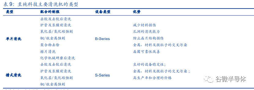
In the field of wet process equipment, the company established an independent semiconductor wet process business department in 2017. The product cavity, equipment platform design and process technology are consistent with the line of the international first-line large manufacturers. The nano water particle technology produced by the advanced two fluids can effectively remove particles and avoid the high cost of megasonic wave. According to the company's announcement, the company's current wet process equipment has two types: trough type and monolithic type (8-12 reaction chamber), which can provide all wet processes to 28 nm nodes; In the first half of this year, the company has received formal orders for four sets of machines and multiple processes in the more advanced 14nm ~ 7Nm technology generation, which will be delivered to the customer's production line for verification in 2022. In terms of technical reserve, the company will continue to invest resources to develop equipment (such as multi reaction chamber, 18 chamber, etc.) that meets high-level process applications. The subsystems of the company's wet process equipment include chemical liquid circulation system, temperature control system, transmission system, automatic control system, communication system, sensor control system, gas flow field design, reaction chemical liquid recovery ring design, etc.
From the perspective of customers, the company's wet equipment has entered the first-line users, including SMIC international, Huahong group, Changxin storage, Huawei, China Resources, Yandong, Taiwan Lijing, etc., all of which are leaders in the downstream industry. Among them, the company's single-chip wet cleaning equipment has won many orders from important domestic users, and high-temperature sulfuric acid, crystal back cleaning, post stage degumming, and long film front single-chip machines have been selected, further filling the gap of domestic equipment in the field of wet cleaning.
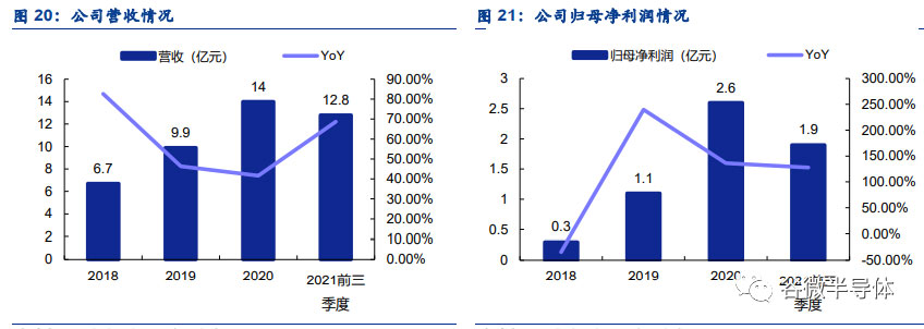
From the company's financial data, the company's overall performance shows a high-speed growth trend, from 670 million in 2018 to 1.4 billion yuan in 2020; The company's net profit attributable to the parent increased from 30 million yuan in 2018 to 260 million yuan in 2020. In the first three quarters of 2021, the company realized a total operating income of 1.283 billion yuan, a year-on-year increase of 68.71%. The net profit attributable to the parent was 188 million yuan, with a year-on-year increase of 127.96%. After deducting the non attributable net profit of 80.5268 million yuan, with a year-on-year increase of 97.55%. In terms of orders, according to the data of the company's interactive platform, as of the reporting period of the third quarter of 2021, the current orders of the wet process Department of the company have exceeded 800 million, of which the orders of new single-chip equipment have exceeded 400 million yuan. The orders of the first three quarters have exceeded the level of the whole year of 2020.
In October 2021, the company's subsidiary Zhiwei technology introduced shareholders including large fund phase II, SMIC Juyuan, equipment and materials fund, Yuanzhi Xinghuo, Xinxin Dingxiang and so on through capital increase and share expansion. The list of shareholders of this war investment covers domestic excellent semiconductor investment funds, indicating that the market is optimistic about the future development prospects of the company. Through this capital increase, the company not only strengthens its capital strength, but also helps the company strengthen industrial cooperation with domestic leading semiconductor companies. The development of the company's semiconductor cleaning equipment is expected to accelerate.
4.2. Shengmei: the leader of semiconductor cleaning equipment in China
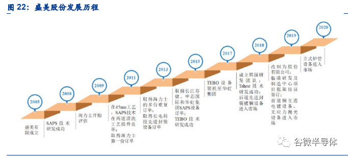
Founded in 2005, shengmei is a semiconductor equipment manufacturer with world leading technology. In 2008, the company successfully developed saps technology. In 2009, SAPS cleaning equipment entered Hynix Korea for product verification. In 2011, the company's saps cleaning equipment for 12 inch 45nm process won Hynix's order for the first time. After 2015, the company successfully obtained orders from Changjiang storage, SMIC international and Huahong group. In 2015 and 2018, the company's Tebo technology and Tahoe technology were successfully developed, and the technology and product line in the field of semiconductor cleaning equipment were more abundant. At present, the company has successfully entered the production line of the world's first-line semiconductor manufacturing enterprises in the field of semiconductor cleaning equipment.
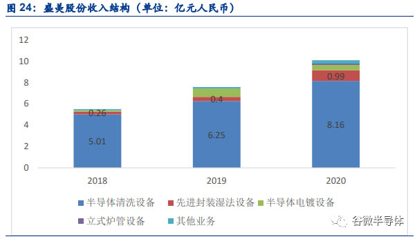
The company's main products include semiconductor cleaning equipment, semiconductor electroplating equipment and advanced packaging wet equipment. The cleaning equipment includes cleaning equipment such as single piece cleaning, trough cleaning and single piece trough combined cleaning; The electroplating equipment includes the front copper interconnection electroplating equipment and the back advanced packaging electroplating equipment for chip manufacturing. In addition, the company has also developed wet etching equipment, coating equipment, developing equipment, degumming equipment, stress-free polishing equipment and vertical furnace tube series equipment for advanced packaging.
In the field of cleaning equipment, based on independent innovation, the company has successfully developed the world's first saps, Tebo megasonic cleaning technology and Tahoe single-chip groove combined cleaning technology through years of technology research and development and process accumulation, which can be applied to the wafer cleaning field of 45nm and below technology nodes, effectively solve the problems of organic contamination and particle cleaning after etching, and greatly reduce the use of chemical reagents such as concentrated sulfuric acid, While helping customers reduce production costs, we also meet the requirements of energy conservation and emission reduction.
According to the company's financial data, the company's revenue showed a rapid growth trend, from 550 million yuan in 2018 to 1.01 billion yuan in 2020, and the revenue nearly doubled. In terms of profitability, the company's net profit attributable to the parent increased from 90 million yuan in 2018 to 200 million yuan in 2020, and the net profit attributable to the parent more than doubled. According to the data of the prospectus, the company realized a revenue of 1.088 billion yuan in the first three quarters of this year, with a year-on-year increase of 78.89%, and a net profit attributable to the parent company of 149 million yuan, with a year-on-year increase of 21.43%. The main reason for the continued high growth of the performance is the high prosperity of the semiconductor equipment market and the domestic substitution demand.
4.3. North Huachuang: leading domestic semiconductor equipment, both single chip and trough cleaning equipment
Beifang Huachuang was founded in 2001 and was formed by the strategic reorganization of Beijing Seven Star Huachuang and Beifang microelectronics in 2016. Its headquarters is located in Beijing; North Huachuang is mainly engaged in semiconductor equipment, vacuum equipment, new energy lithium battery equipment and precision components, providing solutions for semiconductor, new energy, new materials and other fields. North Huachuang has four core business clusters: semiconductor equipment business group, vacuum equipment business group, new energy lithium battery business group and precision components business group. In terms of semiconductor equipment, the company has established a rich and competitive product system, which is widely used in semiconductor, new materials, new energy and other fields. Etching machine, PVD, CVD, ALD, oxidation / diffusion furnace, annealing furnace, cleaning machine and other products have been applied in mass production in the integrated circuit and pan semiconductor fields, forming a multi variety and cross domain product platform for semiconductor equipment and becoming an advanced semiconductor equipment supplier in China.
In terms of semiconductor cleaning, North Huachuang can provide various types of single-chip cleaning equipment and trough cleaning equipment, which have been widely used in integrated circuits, semiconductor lighting, advanced packaging, micro electromechanical systems, power electronics, compounds and power devices. In 2018, North Huachuang acquired akrion, an American semiconductor cleaning equipment company, to improve the cleaning equipment production line. At present, the company's main cleaning equipment products are single chip and trough cleaning equipment, which can be used for chip manufacturing with 65nm and 28nm technology nodes.
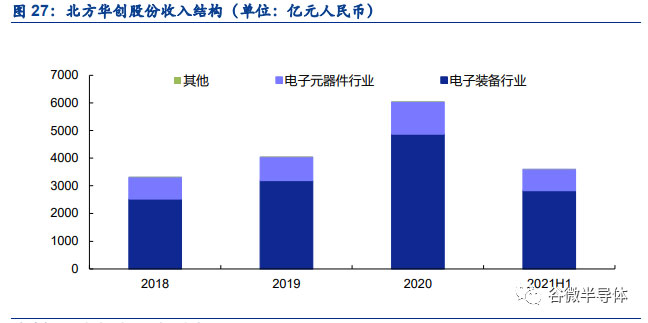
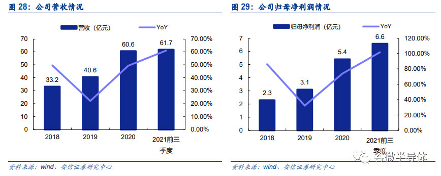
From the company's financial data, the company's performance shows a rapid growth trend, from 3.32 billion yuan in 2018 to 6.06 billion yuan in 2020; The company's net profit attributable to the parent increased from 230 million yuan in 2018 to 540 million yuan in 2020. In the first three quarters of 2021, the company's operating revenue and net profit attributable to the parent increased significantly year-on-year, and the net profit attributable to the parent was close to the upper limit of the previous performance guidance. The company's revenue in the first three quarters increased significantly year-on-year mainly because of the high popularity of the semiconductor market scene, and the expansion of capital expenditure by wafer factories one after another led to better equipment demand. In addition, as of Q3, the company's contract liabilities were 5.5 billion yuan, a year-on-year increase of + 81% and a month on month increase of + 16%, mainly due to the increase in sales orders and the increase in contract advance receipts received from customers.
Source: Anxin securities Authors: Ma Liang, Guo Wang (the above articles are reprinted and do not represent the views of Guwei semiconductor. If there are copyright issues, please contact us for handling)
Business consultation hotline
| Contact us
| 
Follow official account |
 Address: No. 116-8, Xinkai South Road, development zone, Nantong City, Jiangsu Province
Postal Code:226010
Address: No. 116-8, Xinkai South Road, development zone, Nantong City, Jiangsu Province
Postal Code:226010  Email: tuhui@go-wellsemi.com
 TEL:0513-85708666